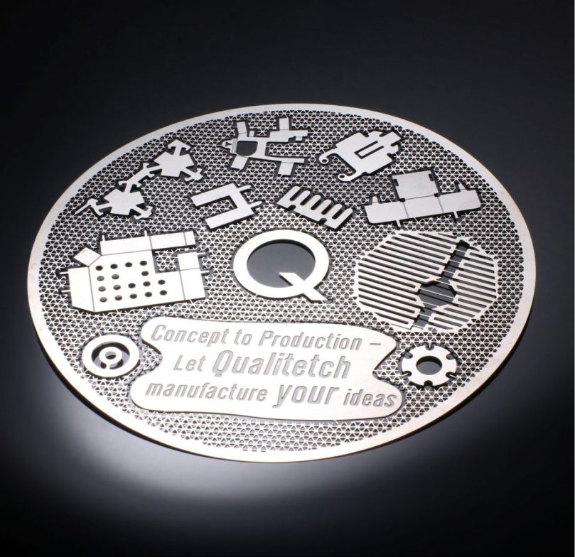
Chemical etching or Photo etching as it’s otherwise known, is a method widely used in many industries, including electronics, to create intricate metal components such as lead frames. These frames play a role in electronics by providing support and electrical connections for semiconductor devices like integrated circuits (ICs) and transistors. Let’s look at why chemical etching stands out as a preferred choice for manufacturing metal lead frames for electronics;
- Precision and Accuracy; Chemical etching is a perfect manufacturing process for producing accurate metal lead frames with very intricate geometries. This precision is vital in the electronics sector, where components need to fit to ensure performance and reliability.
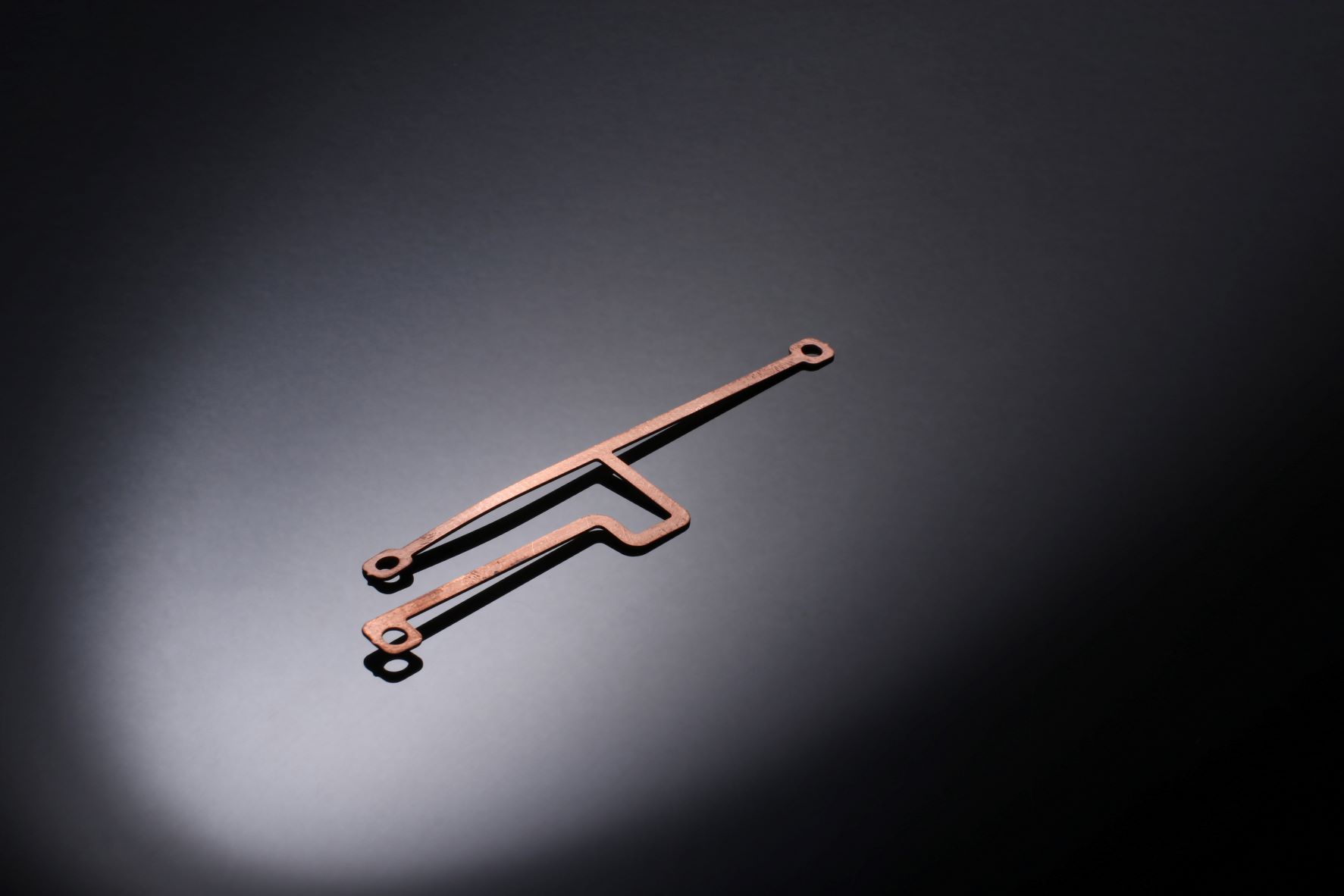
- Detailed Designs; The process of chemical etching enables the fabrication of lead frames with designs, including features and tight tolerances. This capability is essential for meeting the evolving demands of devices that are becoming increasingly compact and specialised.
- Burr Free and Stress Free; Unlike machining methods chemical etching yields burr free and stress free lead frames. This quality is especially beneficial in electronics manufacturing since burrs and stresses can impact the performance and reliability of semiconductor devices.
- Material Flexibility; Chemical etching is compatible with an array of metals used in frame production, such, as copper, copper alloys and various grades of stainless steels to name just a few. The adaptability of chemical etching enables manufacturers to select the material for their specific application needs considering factors such, as conductivity, resistance to corrosion and overall cost.
- Cost Efficiency; The etching process lends itself to substantial cost savings in large scale production whilst also being perfect for prototype designs that may require changes quickly. As once the etching mask artwork is ready, the actual etching process proves itself to be swift and effective, making it a viable option for manufacturing metal lead frames in bulk or smaller volume quantities or first off’s for approval.
- Scalability; Chemical etching demonstrates scalability catering to both small batch prototyping and mass production of metal lead frames. This scalability feature allows companies to promptly adjust to fluctuations in demand and efficiently increase production levels as required ensuring availability of components in the market.
- Environmental Friendliness; In comparison, to other manufacturing methods, chemical etching is generally recognised as an eco-manufacturing process. The chemicals utilised during etching procedures can often be reused, resulting in environmental impact when supported by proper waste management strategies.
- Versatility; Chemical etching provides customisation capabilities and flexibility that enable manufacturers to tweak designs and undergo rapid iterations during the product development stage. This flexibility is crucial, in the fast paced electronics sector, where creativity and speed to market play a role in achieving success.
- Quality Assurance; Chemical etching provides control over the production process ensuring quality and consistency of metal lead frames. This level of quality assurance is crucial for meeting the standards of the electronics industry and providing components to clients.To sum up chemical etching stands out as a favoured manufacturing technique, for crafting metal lead frames in the electronics field because of its accuracy, adaptability, cost efficiency and eco-friendly nature. By capitalising on the advantages of chemical etching, manufacturers can create top quality lead frames that fulfil the demands of required by the electronic devices industry.